
In the intricate tapestry of modern technology, transistors are the unseen threads that bind our digital world together — tiny switches that flicker billions of times per second to make our devices think, communicate, and respond. They are the quiet engines of our connected lives, and for decades, scientists have pushed their limits, dreaming of transistors that are smaller, faster, and more efficient than ever before. Yet even in the realm of cutting‑edge research, there is wisdom in pausing to reflect on how we measure success. Recent findings from engineers at Duke University suggest that, in many laboratory studies of next‑generation transistor designs, reported performance may have been overestimated due to the test architectures used — a revelation that invites both humility and deeper insight into the path toward future computing.
For nearly twenty years, researchers have explored the promise of two‑dimensional (2D) semiconductors — materials a few atoms thick — as potential successors to silicon. In laboratory settings, these materials have often shown remarkable promise, suggesting pathways to devices that could operate at higher speeds and with greater energy efficiency than conventional silicon. However, much of this optimism was built on measurements using a configuration known as the back‑gated architecture, which, while convenient for early testing, may not represent the performance that real‑world devices will achieve. The latest study led by Professor Aaron Franklin and his team reveals that this testing method can subtly inflate reported performance, painting an overly rosy picture of how soon 2D materials might transform commercial electronics.
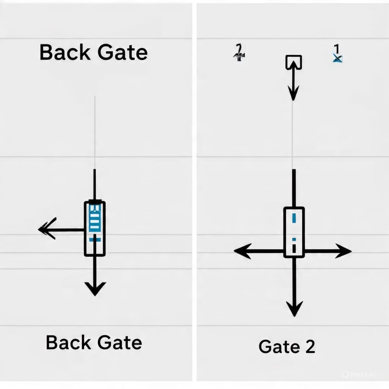
In the back‑gated setup, all transistor components are built onto a single silicon base, allowing rapid experimentation but also creating what scientists call contact gating — an effect in which the gate voltage influences not only the transistor’s channel but also the regions under its metal contacts. This effect can artificially lower resistance and boost current in ways that would not be feasible in devices built for commercial use. As Dr. Franklin explains, it’s like training for a race on a downhill slope and then expecting the same speed on flat terrain: the performance appears high in the lab, but the conditions are not the same as those in real‑world applications.
To probe the extent of this inflation, the researchers compared traditional back‑gated designs with a symmetric dual‑gate architecture that separates control of the transistor channel from the contact regions. In direct comparisons, the performance of the devices with contact gating was starkly higher — sometimes by several times — than that of devices measured without this effect. At very small scales relevant for future technologies, the impact of contact gating became even more pronounced, underscoring how sensitive these measurements can be to experimental design.
This finding has important implications for the broader field of transistor research. With hundreds of published studies relying on back‑gated measurements, many reported performance claims may need reevaluation in the context of architectures that reflect what can realistically be achieved in future chip designs. As the semiconductor industry seeks to move beyond silicon and develop technologies that can support ever‑increasing computing demands, clear and comparable performance benchmarks will be essential to guide innovation.
At a time when advances in semiconductors are closely tied to breakthroughs in artificial intelligence, communications, and portable computing, this study serves as a gentle reminder that measurement methods are as important as the materials themselves. Honesty and precision in testing not only clarify what is possible, but also help ensure that expectations — for researchers, companies, and the public — align with reality.
In clear terms, researchers found that many lab tests of next‑generation 2D transistor performance use designs that overstate how these devices would behave in practical applications. By comparing these conventional test setups with alternative architectures that avoid contact gating, engineers illustrated that reported performance may be significantly inflated, suggesting greater caution and rigor in future evaluations.
AI Image Disclaimer “Visuals are created with AI tools and are not real photographs, intended for representation only.”
Source Check — Credible Media Names Mirage News Duke Pratt School of Engineering ScienceDaily EurekAlert! Yahoo News
Published by Banx Network. This article is part of the Banx decentralized media programme, powered by the BXE token on the XRP Ledger.