

Key Highlights
- New Technology:Caltech engineers create a fingernail-sized chip for light separation.
- Efficiency:The chip achieves low loss in separating light into individual beams.
- Applications:Potential uses in telecommunications, sensing, and quantum computing.
[Innovative Technology]
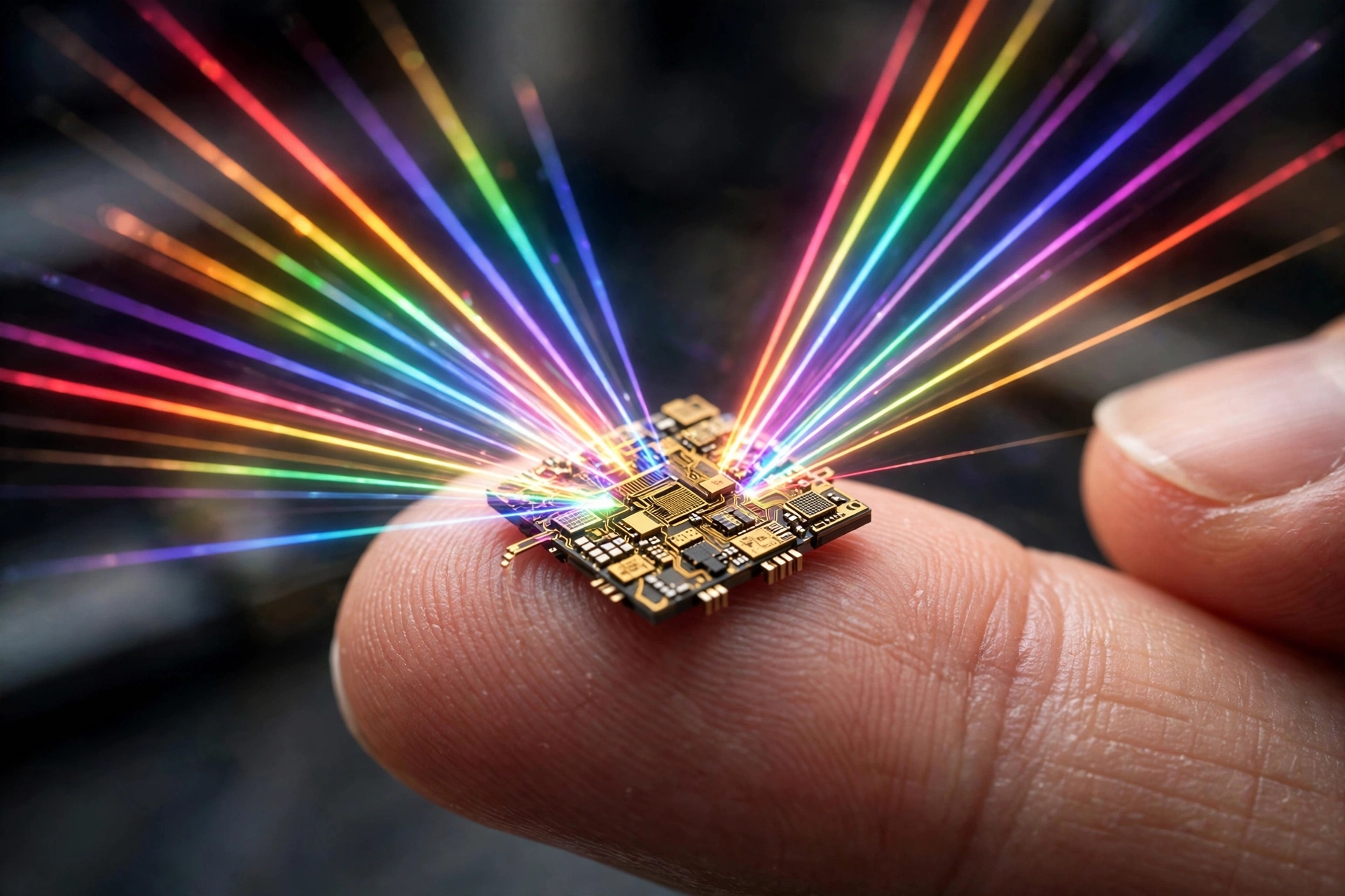
Engineers at the California Institute of Technology have unveiled a groundbreaking chip, no larger than a fingernail, capable of separating mixed light into distinct beams, each representing a single color. This innovative device, detailed in the journal Nature Photonics, marks a significant leap forward in photonics technology, with promising implications for telecommunications, sensing, and quantum computing.
The chip operates on the principle of wavelength demultiplexing, a process traditionally performed by larger, more expensive devices known as demultiplexers in fiber-optic communications. The team, led by Andrei Faraon, has harnessed a metasurface—a flat, nanostructured material that precisely manipulates light—to achieve this function in a compact form factor. This advancement not only reduces the size of the technology but also enhances its accessibility for various applications.
[Efficiency and Performance]
One of the standout features of this new chip is its remarkable efficiency. Researchers have reported that the device can effectively separate light into individual channels with minimal loss, ensuring that the majority of the light entering the chip exits as intended. This characteristic is crucial for practical applications, as signal loss can significantly impair performance and inflate costs. Furthermore, the chip's compatibility with existing semiconductor manufacturing processes suggests that it could be mass-produced and seamlessly integrated into other photonic systems.
[Potential Applications]
The potential applications for this technology are extensive. In the realm of telecommunications, the chip could facilitate the development of more compact and efficient transceivers, enabling greater data transmission over existing fiber networks. In environmental and medical sensing, it could allow for the detection of specific wavelengths of light with unprecedented sensitivity, paving the way for innovative sensor technologies. Additionally, in quantum computing, the chip could play a vital role in routing and manipulating single photons, which are essential carriers of quantum information.
[Combining Nanotechnology and Photonics]
The research exemplifies the powerful synergy between nanotechnology and photonics. The metasurface at the core of the chip consists of millions of tiny structures, each meticulously designed to interact with light in a specific manner. By arranging these structures in a precise configuration, the researchers have successfully created a device that functions as a wavelength separator without the need for bulky optics or complex assembly processes.
[Future Prospects]
While the chip is not yet ready for commercial use, ongoing refinements and performance enhancements are underway. This proof of concept represents a significant milestone, suggesting that the future of photonics may be characterized by smaller, more cost-effective, and integrated technologies than previously envisioned. The fingernail-sized chip serves as a reminder that transformative innovations often come in surprisingly compact forms.
AI Image Disclaimer: The images in this article are generated by artificial intelligence and are for illustrative purposes only; they do not depict the actual chip, the researchers, or the specific laboratory.
Published by Banx Network. This article is part of the Banx decentralized media programme, powered by the BXE token on the XRP Ledger.