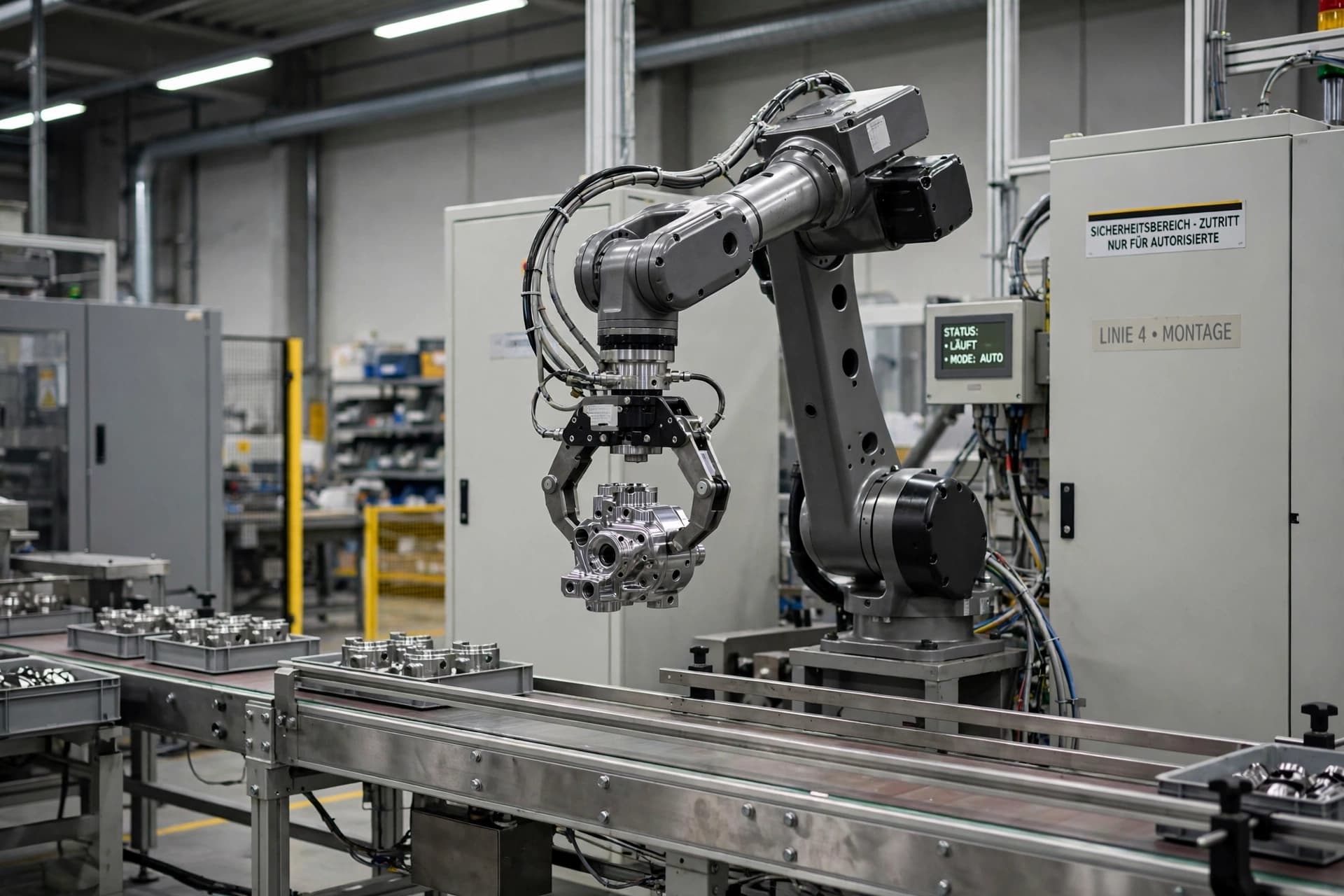
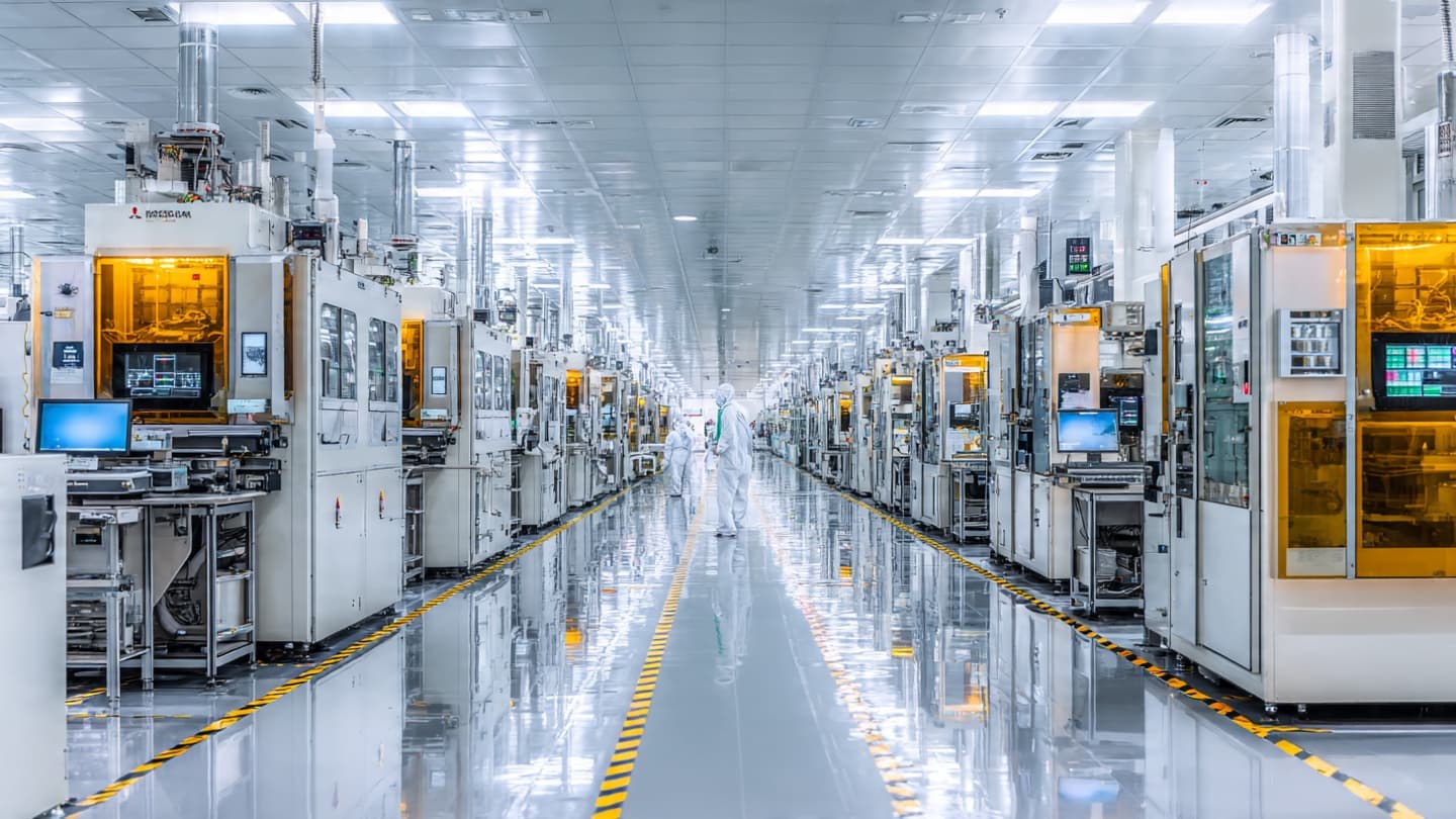
Inside the semiconductor industry, some of the most consequential changes happen far from the finished chip. They take place inside machines that appear almost impossibly precise, where light, optics, materials, and engineering come together to create patterns measured on a microscopic scale.
China has begun mass production of a domestically developed immersion deep-ultraviolet lithography system, according to reporting by Reuters. The development represents another step in Beijing’s effort to strengthen its domestic semiconductor manufacturing capabilities and reduce reliance on foreign equipment.
Lithography is one of the central processes in semiconductor manufacturing. It allows manufacturers to transfer extremely small patterns onto silicon wafers, creating the structures that eventually become transistors and other components inside modern chips.
The technology involved is not the same as the most advanced extreme-ultraviolet lithography used for cutting-edge semiconductor production. Nevertheless, DUV systems remain widely used for many types of chips and industrial applications, making domestic access to such equipment strategically important for a large manufacturing economy.
China’s semiconductor industry has faced restrictions on access to some advanced foreign technologies and equipment. Those restrictions have encouraged domestic companies and research institutions to invest more heavily in developing alternatives and strengthening local supply chains.
The effort is part of a broader transformation within China’s technology sector. Semiconductor manufacturing requires far more than a single lithography machine. It depends on specialized materials, precision optics, wafer equipment, chemical processes, software, testing systems, and highly trained engineers.
Building these capabilities domestically is therefore a long process. Progress in one area can create opportunities for advances elsewhere, while limitations in another component can still constrain the performance of an entire manufacturing system.
The significance of domestic lithography also extends beyond the semiconductor industry itself. Chips are used throughout modern economies, from automobiles and telecommunications equipment to industrial machinery, consumer electronics, and artificial-intelligence systems.
China’s push toward greater semiconductor self-sufficiency consequently reflects a desire to make its technology ecosystem more resilient. Rather than relying entirely on imported equipment, manufacturers are seeking to develop more of the machinery and expertise required to produce chips inside the country.
The emergence of domestic lithography does not mean that China has eliminated the technological gap with the world’s leading semiconductor-equipment producers. Advanced chip manufacturing remains highly complex and competitive. But the movement toward mass production demonstrates that China continues to build capabilities step by step.
In the quiet rooms where lithography machines operate, the global semiconductor competition becomes something physical: lenses, light, silicon, and machines working together. China’s latest development adds another piece to that intricate landscape, showing how the race for technological independence increasingly begins with the equipment used to make the equipment of tomorrow.
AI Image Disclaimer: These images were generated with AI as conceptual illustrations and do not depict verified photographs of specific equipment.
Sources: Reuters ASML Semiconductor Industry Association China Semiconductor Industry Association
Published by Banx Network. This article is part of the Banx decentralized media programme, powered by the BXE token on the XRP Ledger.